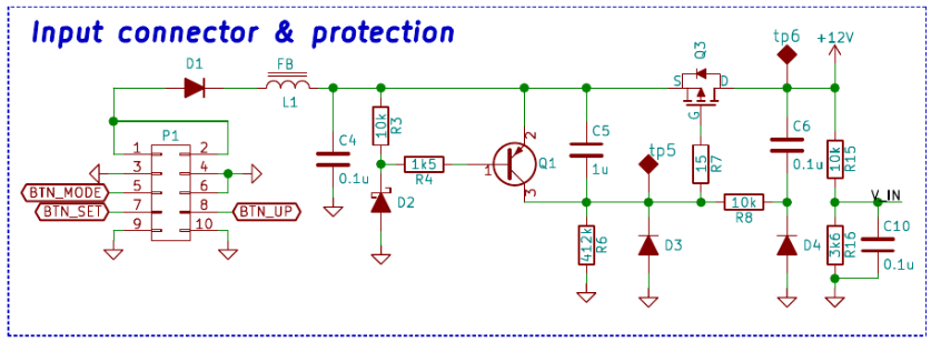
Input protection
The circuit is protected against four undesired situations:
- Reverse polarity protection
- Overvoltage
- Undervoltage
- Inrush current
The image below shows the power input circut section, that implements 3 of these four measures.

The connector P1 to the left receives power and button signals from a secondary PCB on the back of the clock that includes the 12V plug and three buttons. Both PCBs are connected via a 10-wire ribbon cable.
-
Reverse polarity protection: This is the simplest. The diode
D1protects against any backward current flow. The drawback is the diode voltage drop (close to 0.5V). If necessary, it can be avoided by using a MOSFET switch like this one. But it wasn’t necessary in this case. -
Overvoltage:
D2is a Zener diode with zener voltage of 14V. When an input voltage above 14.5V (aprox.) is applied to the input,D2conducts current, forcingQ1into saturation (that is, Vce close to zero), thus, switching the P-channel MOSFET transistorQ3off. This way, overvoltage causes the whole circuit to be de-energized. Only the maximum voltage ratings of the input components limit the maximum input voltage, which can be up to 40V. Overvoltage protection is desired since some of the components of the circuit have a maximum voltage rating of 18V. -
Undervoltage: This one is not implemented by the input circuitry. There might be a discrete solution using zeners and transistors to implement undervoltage limits, but it was much easier to do in software. Basically, at start up, the MCU checks all system voltages. If there’s an input voltage lower than nominal 12V, the boost converter won’t be enabled. This way, the boost controller is protected from working with duty cicle very close to 1.
-
Inrush current: Needed for two reasons:
- The current spike produced in the connection process degrades the bulk capacitance in the circuit, and may produce MCU malfunction at start up.
- The quality of the user’s power adapter is unkwnown, and there’s an alarmingly high amount of adapters without converter controller chips. This translates into power adapters not working, or producing big voltage sags in the connection moment, or outputting voltages different than 12V after connecting them. Thus, Inrush Current Limitting (ICL) is a safety measure against weak power sources.
ICL is the most interesting, so it’s explained below.
The goal is to switch on Q3 slowly, in a controlled fashion, so that it remains in active mode (not in saturation) for a short period of time, such that it effectively acts as a resistor. This is achieved by slowly decreasing the Gate voltage (with respect to Source) using the RC filter C5 and R6. As soon as Q3 reaches the threshold voltage, current starts flowing through the transistor and the voltage at TP6 increases. C6 and R8 act as a feedback loop, so when voltage at TP6 increases, current across R6 also increases and Vgs (source-gate voltage) gets regulated. The whole transient effect results in a very nice ramp voltage from zero to 12 volts at TP6 (the +12V rail), lasting a some milliseconds. This is shown in the image below.

- Yellow trace: Input voltage rail (from power adapter).
- Blue trace: MOSFET gate voltage (with respect to ground).
- Purple trace: 12V rail (TP6).
R15 and R16 sample the input voltage to be read by the MCU.